skype:
skype:


Common LCD interfaces are RGB, LVDS, MiPi
In addition to the above three interfaces, there are some other interfaces such as i2c and SPI. The small screen of the MCU interface is relatively simple, so I will not describe it here.
1. RGB interface
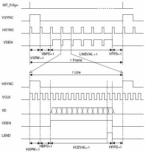
The RGB color mode is a color standard in the industry. It obtains various colors by changing the three color channels of red®, green (G), and blue (B) and superimposing them with each other. RGB is the color representing the three channels of red, green, and blue. This standard includes almost all the colors that human vision can perceive, and it is one of the most widely used color systems. The TTL output interface of the driver board generally contains three types of signals: RGB data signals, clock signals and control signals. Clock signal Refers to the pixel clock signal, which is the basis for transmitting data and reading data signals. When using odd/even pixel dual-channel transmission of RGB data, different output interfaces use pixel clock methods differently. Some output interfaces for odd/even pixel data share one pixel clock signal, and some output interfaces for odd/even two channels respectively set odd pixel data clock and even pixel clock signals to meet the needs of different LCD panels. control signal The control signal includes a data enable signal (or effective display data strobe signal) DE, a horizontal synchronization signal HS, and a vertical synchronization signal VS.
2.LVDS interface
LVDS (Low Voltage Differential Signalin) is a low-amplitude differential signal technology. It uses very low amplitude signals (about 350mV) to transmit data through a pair of differential PCB traces or balanced cables. It can transmit serial data at speeds up to thousands of Mbps. Because the voltage signal amplitude is low and it is driven in a constant current source mode, it only generates extremely low noise, consumes very little power, and even the power consumption is almost unchanged regardless of the frequency. In addition, because LVDS transmits data in a differential manner, it is not susceptible to common mode noise.
The reason why LVDS has become the preferred signal form of high-speed I/O interface to solve the limitation of high-speed data transmission is because it has advantages in transmission speed, power consumption, anti-noise, EMI, etc.
① High-speed transmission capability. In the LVDS standard defined by ANS/EIA/EIA-64, the theoretical limit rate is 1.923Gbps. The working mode of constant current source mode and low swing output determines the high-speed driving capability of IVDS.
②Low power consumption characteristics. LVDS devices are implemented using CMOS technology, and CMOS can provide lower static power consumption; when the drive current of the constant current source is 3.5mA, the power consumption of the load (100Ω terminal matching) is only 1.225mW; the power consumption of LVDS is Constant, unlike the dynamic power consumption of CMOS transceivers that rise with respect to frequency. The drive design of the constant current source mode reduces the system power consumption and greatly reduces the influence of frequency components on power consumption. Although the power consumption of CMOS is lower than that of LVDS when the speed is low, as the frequency increases, the power consumption of CMOS will gradually increase, and eventually it will consume more power than LVDS. Generally, when the frequency is equal to 200MSps, the power consumption of LVDS and CMOS is roughly the same.
③The power supply voltage is low. With the development of integrated circuits and the requirement for higher data rates, low-voltage power supply has become an urgent need. Lowering the supply voltage not only reduces the power consumption of high-density integrated circuits, but also reduces the heat dissipation pressure inside the chip, which helps to improve the integration. LVDS drivers and receivers do not depend on specific power supply voltage characteristics, which determines that it occupies the top in this regard.
④Strong anti-noise ability. The inherent advantage of the differential signal is that noise is coupled to a pair of differential lines in a common mode, and subtracted in the receiver, thereby eliminating noise, so LVDS has a strong ability to resist common mode noise.
⑤ Effectively suppress electromagnetic interference. Because the polarities of the differential signals are opposite, the electromagnetic fields radiated by them can cancel each other out. The tighter the coupling, the less electromagnetic energy leaked to the outside world, which reduces EMI.
⑥ Precise timing positioning. Because the switch change of the differential signal is at the intersection of the two signals. Unlike ordinary single-ended signals, which rely on high and low thresholds The voltage judgment is less affected by the process and temperature, can reduce the error in the timing, and is beneficial to the effective transmission of high-speed digital signals.
⑦ Adapt to a large range of ground plane voltage changes. The LVDS receiver can withstand at least ±1V of the ground voltage change between the driver and the receiver. Since the typical bias voltage of the IVDS driver is +1.2V, the sum of the ground voltage change, the driver's bias voltage, and the lightly coupled noise, is a common-mode voltage at the receiver input relative to the driver's ground. When the swing does not exceed 400mV, the common-mode range is +0.2V+2.2V, and in general, the input voltage range of the receiver can vary within 0V+2.4V. The LVDS signal consists of data differential and clock differential signals. As shown below
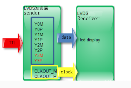
Single channel 6-bit data (if it is a 6-bit Y3M/P group of red lines, there is no) There are 4 sets of differential lines, 3 sets of signal lines, and one set of clock lines. Y0M, Y0P, Y1M, Y1P, Y2M, Y2P, CLKOUT_M, CLKOUT_P
Data bits: single-channel 6-bit data, dual-channel 6-bit data, single-channel 8-bit data, dual-channel 8-bit data, single-channel 10-bit data, dual-channel 10-bit data Dual channel means that the LCD has two sets of data lines and clock lines
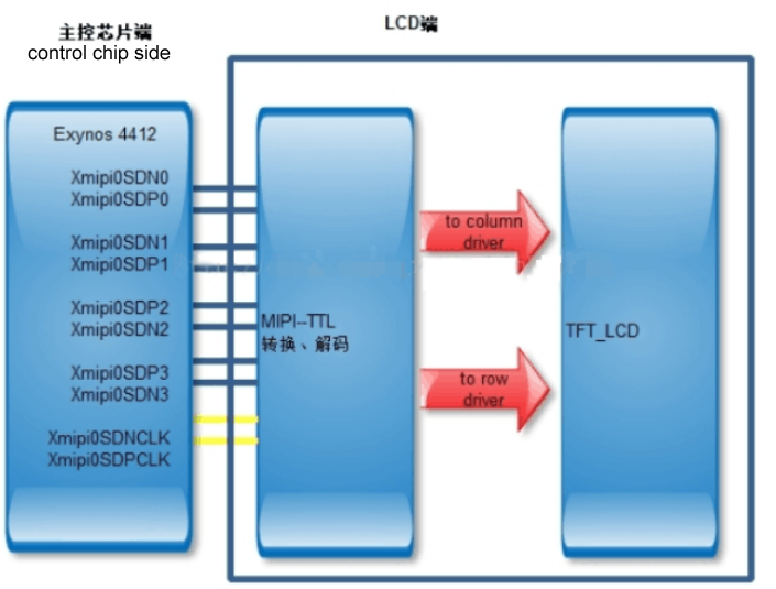
3.MIPI
A master control output differentially controls the LCD terminal, The main composition is: 1 set of clock differential + at least one set of differential data lines There is a mipi decoder inside the lcd which can support RGB decoding.